
The semiconductor industry is currently navigating its most significant architectural shift in decades. For over fifty years, the trajectory of computing power followed a predictable path defined by Moore’s Law: the doubling of transistors on a monolithic piece of silicon every two years. However, as transistors approach atomic scales, the physics of shrinking them further has become prohibitively expensive and technically daunting. The industry has reached a crossroads where the traditional “single-chip” approach is hitting a wall of diminishing returns.
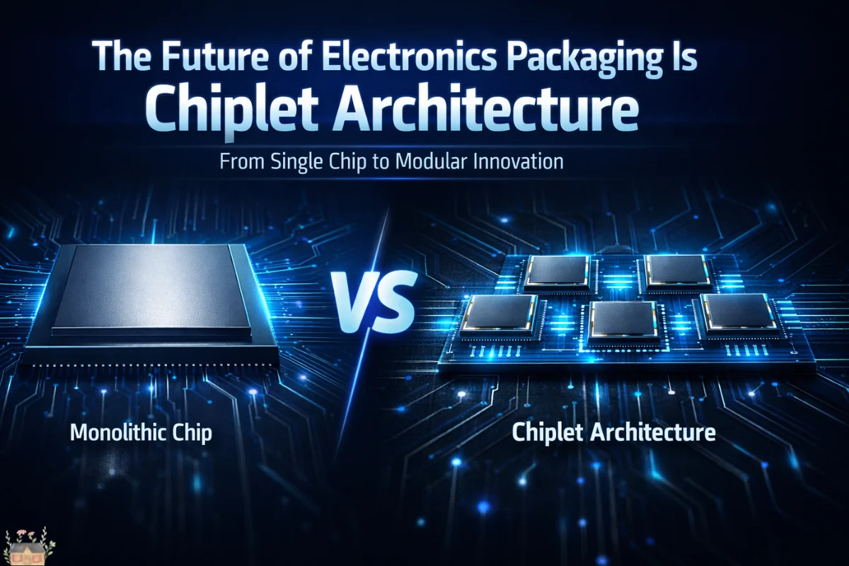
Engineers and manufacturers are now pivoting toward a modular philosophy. This transition confirms that the future of electronics packaging is chiplet architecture, a design methodology that breaks a large, complex processor into smaller, functional components that work together as a single unit. This shift is not merely a trend; it is a fundamental necessity for the next generation of high-performance computing, artificial intelligence, and consumer electronics.
Understanding the Transition from Monolithic to Modular Design
To appreciate the rise of chiplets, one must first understand the limitations of the monolithic “System on Chip” (SoC). In a traditional SoC, every component—the CPU cores, the graphics engine, the memory controller, and the I/O—is fabricated on a single continuous piece of silicon.
While this approach minimizes the distance data must travel, it creates a massive “all or nothing” risk. If a single microscopic defect occurs during the manufacturing of a large 800mm² chip, the entire unit may have to be discarded. As chips grow larger to meet the demands of modern AI workloads, these “yield” issues become a financial black hole.
Chiplet architecture solves this by disaggregating the design. Instead of one giant chip, designers create smaller “chiplets” optimized for specific tasks. These are then combined on an advanced packaging substrate.
The Economic Logic of Chiplets
Manufacturing costs do not scale linearly with chip size; they scale exponentially. A chip that is twice as large is often more than twice as expensive to produce because the probability of a fatal defect increases. By using smaller chiplets, manufacturers achieve much higher yields. Furthermore, not every part of a processor needs to be built using the most expensive, cutting-edge “node” (like 3nm).
For example, a processor might feature high-performance CPU cores built on a 3nm process, while the I/O and communication components—which do not benefit as much from shrinking—are built on a more mature and cost-effective 7nm process. This “heterogeneous integration” is a cornerstone of why the future of electronics packaging is chiplet architecture.
Technical Foundations: Interconnects and Advanced Packaging
The primary challenge of a modular design is communication. When you split a processor into pieces, those pieces must talk to each other at lightning speed with minimal power consumption. If the connection between chiplets is too slow, the performance gains of the silicon are lost to “latency.”
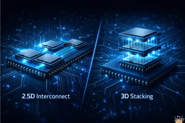
This has birthed a new era of advanced packaging technologies. We are moving beyond simple printed circuit boards toward sophisticated 2.5D and 3D integration techniques.
2.5D Packaging and Silicon Interposers
In 2.5D packaging, chiplets are placed side-by-side on a “silicon interposer.” This interposer acts as a high-speed highway, allowing data to move between modules far faster than traditional traces on a motherboard. This is the technology currently powering the world’s most advanced AI GPUs and data center processors.
3D IC (Integrated Circuits)
3D packaging takes the concept further by stacking chiplets vertically. By placing memory directly on top of a logic die (using technologies like Through-Silicon Vias or TSVs), the distance data travels is reduced to micrometers. This vertical integration provides a massive boost in bandwidth and energy efficiency, which is critical for mobile devices where space is at a premium.
Read Also: DPSIT: Digital Payment Security & Trust Architecture
Comparing Architectures: Monolithic vs. Chiplet
The following table outlines the fundamental differences between the traditional approach and the modular future.
Driving Forces: Why Now?
Several market forces are converging to make the adoption of chiplets inevitable.
1. The AI Explosion
Artificial Intelligence requires massive amounts of parallel processing and enormous memory bandwidth. Training a Large Language Model (LLM) involves moving terabytes of data between memory and logic units. Monolithic chips simply cannot grow large enough to house all the necessary components for next-gen AI. Chiplets allow companies to “tile” processors together, creating massive computing clusters on a single package.
2. Thermal Management
When all heat-generating components are packed onto a single piece of silicon, thermal “hotspots” become a major bottleneck. Chiplets allow for better spatial distribution of heat. Designers can place the hottest logic components further apart or intersperse them with less heat-intensive I/O units, making cooling solutions more effective.
3. Sustainability and Cost
The “Silicon Wastage” problem is real. As the industry moves toward 2nm and beyond, the cost per wafer is skyrocketing. The ability to reuse chiplet designs across different product lines—for example, using the same I/O chiplet in both a laptop processor and a server processor—dramatically reduces R&D waste and hardware scrap.
The Role of Standardization: UCIe and Beyond
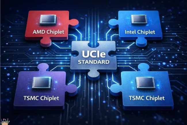
For a modular ecosystem to thrive, the industry needs a common language. Historically, companies like AMD, Intel, and TSMC developed their own proprietary ways for chiplets to communicate. However, the true potential of the “future of electronics packaging is chiplet architecture” lies in a “plug-and-play” ecosystem where a designer could theoretically buy a CPU chiplet from one vendor and an AI accelerator chiplet from another.
The Universal Chiplet Interconnect Express (UCIe) is an industry-standard specification that aims to define the physical layer and protocol for chiplet communication. With the backing of major tech giants, UCIe is paving the way for a competitive marketplace of modular silicon components.
Challenges on the Horizon
While the benefits are clear, the transition to chiplets is not without hurdles. The complexity of the supply chain increases significantly. Instead of testing one chip, manufacturers must now test multiple chiplets and then test the final “Known Good Die” (KGD) after it has been packaged.
Furthermore, the design tools (EDA software) must evolve to handle the complexities of 3D thermal modeling and signal integrity across multiple substrates. The industry is currently in a “learning phase” regarding the long-term reliability of advanced packaging under the stress of thermal cycling.
Read Also: Crackstube Explained: Risks, Safety & Legal Alternatives
Future Outlook: The “Lego” Era of Computing
Looking ahead, we are entering an era where hardware design looks more like building with Legos than carving from a single stone. We can expect to see:
-
Custom Silicon for Small Players: Startups will be able to design a single specialized chiplet and integrate it with off-the-shelf “base” chiplets, reducing the entry hurdles for custom silicon development.
-
Edge Computing Breakthroughs: Mobile devices will use 3D stacking to provide “desktop-class” performance by layering specialized neural processing units (NPUs) directly onto image sensors or memory.
-
Rapid Iteration: Companies will be able to update specific parts of a processor (like the security module or the wireless radio) without redesigning the entire CPU.
Summary of Key Takeaways
The transition toward modularity is the most effective response to the physical and economic limits of silicon fabrication. By embracing chiplets, the electronics industry can continue to deliver the performance gains required by modern software while keeping costs manageable and yields high.
-
Yield Improvement: Smaller components lead to fewer wasted wafers.
-
Heterogeneous Integration: Using the right manufacturing process for the right task saves money and improves efficiency.
-
Advanced Packaging: 2.5D and 3D technologies are the new frontier of Moore’s Law.
-
Standardization: Initiatives like UCIe are crucial for a healthy, modular ecosystem.
As we look toward the 2030s, the “single-chip” processor will likely become a relic of the past, found only in the simplest of devices. For everything else, the future is modular, integrated, and layered.
Frequently Asked Questions
1. What exactly is a chiplet?
A chiplet is a functional block of integrated circuitry that forms part of a larger integrated circuit. Instead of manufacturing a large processor as a single piece of silicon, it is broken into these smaller pieces (chiplets), which are then “stitched” together using advanced packaging techniques.
2. Why is chiplet architecture better for AI?
AI workloads require immense memory bandwidth and processing power. Chiplets allow for the integration of High Bandwidth Memory (HBM) very close to the logic units using 3D stacking. This reduces the energy required to move data and significantly increases the speed of AI calculations.
3. Is chiplet architecture more expensive for consumers?
Initially, the advanced packaging required for chiplets adds some cost. However, in the long run, it is expected to lower prices for high-end electronics because chiplets improve manufacturing yields and allow companies to reuse older, cheaper manufacturing processes for non-critical components.
4. Does chiplet architecture affect power consumption?
It comes with trade-offs. Moving data between chiplets can consume more power than internal movement, but because chiplets allow for more efficient “specialized” silicon and better thermal management, the overall system efficiency is often higher than traditional designs.
5. When will we see chiplets in everyday devices?
We already are. Many high-end desktop processors and gaming consoles use chiplet-based designs. As packaging technology matures, this architecture will migrate down into mid-range smartphones, tablets, and even IoT devices over the next several years.
6. What is chiplet architecture?
Chiplet architecture is a modular design that breaks a large processor into smaller, specialized pieces of silicon integrated into a single package. This approach increases manufacturing yields and allows for more flexible, cost-effective hardware.
7. What is the future of microelectronics?
The future lies in system-level innovation through 3D stacking and heterogeneous integration, moving beyond transistor shrinking to vertical and modular designs essential for meeting the massive data demands of AI.
Learn about Bảce
For broader information, visit Wellbeing Makeover

Alex Carter is a writer with 10+ years of experience across tech, business, travel, health, and lifestyle. With a keen eye for trends, Alex offers expert insights into emerging technologies, business strategies, wellness, and fashion. His diverse expertise helps readers navigate modern life with practical advice and fresh perspectives.